Researchers develop new semiconductor material
NEXT LEVEL: Researchers have been exploring ‘2D’ materials that are one or a few atoms thick in hopes of overcoming limitations of conventional materials
By Rachel Lin and William Hetherington / Staff reporter, with staff writer


An international research team co-led by National Taiwan University (NTU) professor Chou Yi-chia (周苡嘉) has developed a “2D” semiconductor made of boron, carbon and nitrogen, potentially overcoming a longstanding obstacle in chip research.
The material is a high-performance p-type semiconductor that conducts electricity primarily through positively charged carriers known as “holes,” rather than free electrons, the researchers said.
The material could help address a lack of high-performance p-type semiconductors for 2D electronics and can be produced on two-inch wafers and used to manufacture transistor arrays, they said.
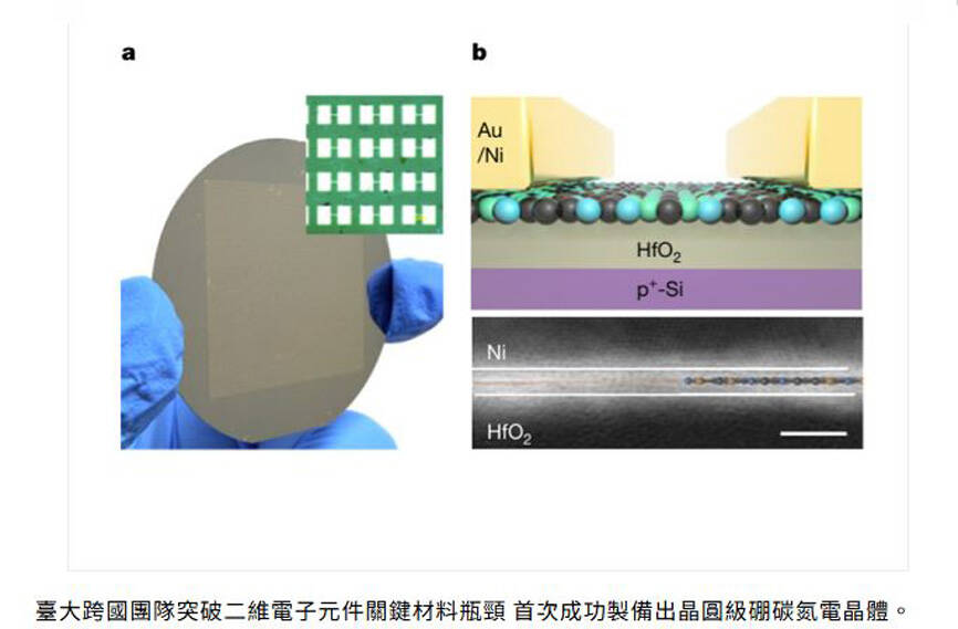
An illustration of a newly developed 2D boron carbon nitride semiconductor is pictured in an undated image.
Photo: Screen grab from National Taiwan University’s Web site
The findings could open new possibilities for next-generation transistors and 3D integrated circuits, they said.
The research was published in the international journal Nature.
As semiconductor components continue to shrink, researchers are increasingly exploring 2D materials that are one or a few atoms thick in hopes of overcoming the limitations of conventional materials and advancing smaller, more efficient electronic devices.
Modern electronic circuits commonly use complementary metal-oxide-semiconductor technology, which requires two types of semiconductors working together: n-type and p-type.
N-type semiconductors conduct electricity primarily through electrons, while p-type semiconductors rely on positively charged holes. Together, the two types help control electrical current and reduce power consumption.
Although researchers have made progress in developing high-performance n-type 2D materials, p-type materials have been more difficult to produce at scale while retaining high-electrical performance. That has created a bottleneck in developing next-generation electronic circuits.
Chou’s team collaborated with researchers from the University of Tokyo and Academia Sinica’s Research Center for Applied Sciences.
Using an atomic-scale materials design approach, they introduced carbon atoms into the lattice of single-layer boron nitride, primarily replacing some of the nitrogen atoms to alter the material’s electronic properties, the team said.
That enabled them to produce a p-type boron-carbon-nitrogen semiconductor with high hole mobility, a measure of how efficiently electrical charge moves through the material.
The team also controlled the chemical reaction pathways of two precursor molecules, enabling the material to be produced on two-inch wafers and used to manufacture transistor arrays, they said.
Tests showed hole mobility of approximately 100cm2 per volt-second and an on-off current ratio of about 100 million to one.
The researchers also evaluated 224 transistors across three batches and found their electrical characteristics to be consistent, they said.
The research was jointly led by Chou of NTU, University of Tokyo professor Vincent Tung (童俊智) and Academia Sinica research fellow Pao Chun-wei (包淳偉). NTU postdoctoral researcher Huang Chang-hsun (黃張勳) was among the study’s co-first authors.
More precise control over the position and number of carbon atoms could enable researchers to further adjust the material’s electrical properties, the team said.
It could also be combined with n-type 2D semiconductors such as molybdenum disulfide to develop next-generation complementary electronic circuits, they added.
KioskNews shows a cleaned-up reading view extracted from the publisher’s page — the original always lives on their site, not ours.