ASML eyes hybrid bonding, report finds, as Chinese firms adopt chip packaging technique
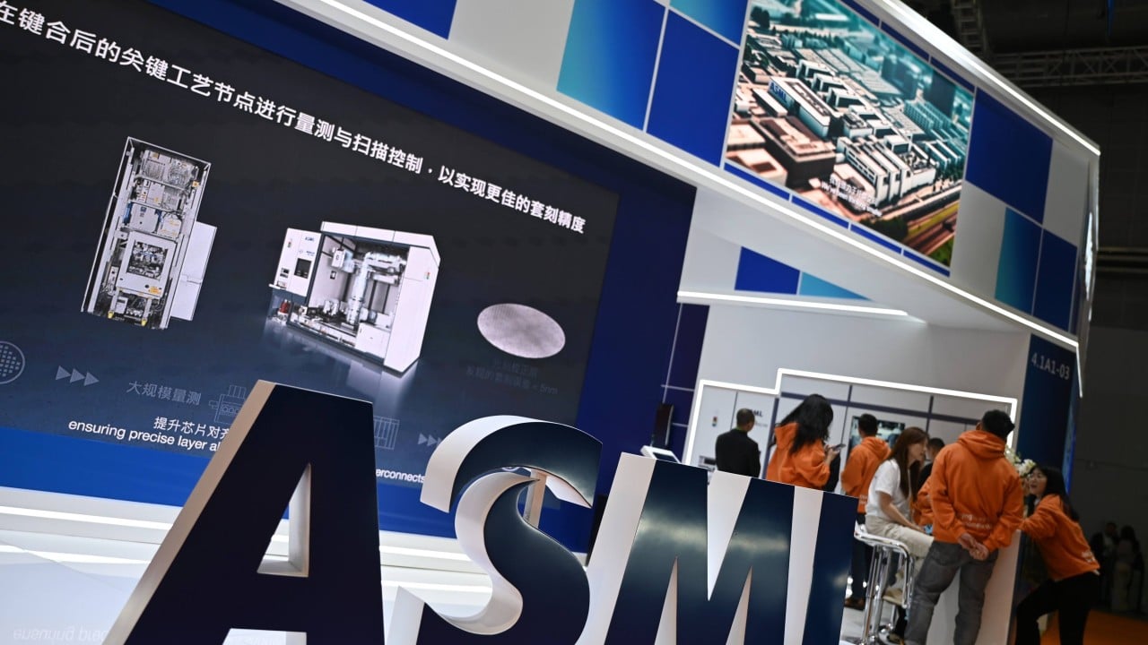
Dutch semiconductor equipment giant ASML is expanding into next-generation hybrid bonding, a technique that creates dense electrical connections by directly joining chips or silicon wafers, according to a new report. Major Chinese companies are also adopting the technology to improve chip performance.
ASML submitted 27 patent families related to hybrid bonding tools between December 2022 and November 2024, according to a report published by semiconductor and AI supply chain research firm SemiAnalysis on Thursday. The number could be higher because of publication delays affecting recent filings, it said.
The filings suggest ASML is moving beyond lithography, a market it dominates, into back-end processes as demand for high-performance chips surges amid the global artificial intelligence boom.
The company had also begun developing the architecture for a hybrid bonder with Dutch technology firms Prodrive Technologies and VDL ETG, according to SemiAnalysis, citing industry media reports.
“We believe ASML could gain an edge in alignment accuracy and particle control for hybrid bonding,” SemiAnalysis said. “These are the two factors that set bonding yield. And ASML has expertise in solving the same problems in lithography.”
The company has not officially announced the extent of its progress on advanced packaging. But CEO Christophe Fouquet said during an April earnings call that the company was “continuing to look for opportunities to support our customers” in hybrid bonding.
ASML told the South China Morning Post by email on Friday that it would “continue to look in which directions [the] 3D integration industry will evolve and to see how this relates to ASML’s roadmap, and where ASML’s expertise can be of added value”.
Hybrid bonding allows ultra-high-density electrical connections and is widely viewed as one of the next major trends in chipmaking. Recent breakthroughs by China’s Huawei Technologies and ChangXin Memory Technologies (CXMT) involved using the technique to improve performance as United States-led export restrictions limit access to some advanced semiconductor equipment.
FULL EVENT: China Future Tech Webinar | The US-China chip war
Under those restrictions, Huawei and CXMT cannot import ASML’s most advanced extreme ultraviolet (EUV) lithography machines.
Hybrid bonding can reduce the thermal resistance in high-bandwidth memory (HBM) stacks by about 30 per cent, according to a September report by Guotai Haitong Securities, which cited Samsung data. Lower thermal resistance can help heat escape more easily, potentially reducing cooling requirements and the need for related investments.
Huawei disclosed new details this week about its flagship Kirin 9050 series, the first mass-produced chip to use its proprietary LogicFolding architecture developed under a framework it calls the Tau Scaling Law. The company said the design integrated more than 50 million hybrid bonds and increased overall transistor density by 53.5 per cent.
CXMT, meanwhile, announced last week that its latest “4F square” dynamic random-access memory architecture used hybrid bonding, which could allow it to increase wafer bit density without relying on advanced EUV lithography.
Despite the potential benefits of the technique, China remained heavily dependent on imported hybrid bonding equipment, particularly advanced machines, according to a separate report by Huaan Securities.
The report noted that domestic equipment manufacturers were stepping up research and development to narrow the gap, with Piotech and Xinhui Lianxin among the leading players.
Piotech’s hybrid bonding equipment generated 136 million yuan (US$20.3 million) in revenue in 2025, up 41.9 per cent from a year earlier, according to its annual report.
Nomura analysts said in a report last week that Huawei’s LogicFolding architecture could drive demand for bonding equipment, as well as Piotech’s mainstay thin-film deposition tools.
KioskNews shows a cleaned-up reading view extracted from the publisher’s page — the original always lives on their site, not ours.