An Epyc trip to Venice: Everything we do and don't know about AMD's 256-core monster chip
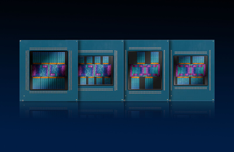
AMD's Venice Epycs mark the chipmaker's biggest architectural shift in CPU design since Rome made its debut all the way back in 2019. What's more, AMD's Zen 6-based product stack is shaping up to be the broadest CPU portfolio ever, spanning general purpose, HPC, AI, and eventually consumer platforms.
AMD isn't quite ready to spill all the beans on its 6th-gen Zen cores, but at this point there's less we don't know about Venice than we do.
Late last week, AMD gave us a bit more to chew on with a whitepaper [PDF] clearly aimed at quashing marketing juggernaut Nvidia's narrative around its Vera CPUs. We'll dive into the performance claims raised in the white paper in a bit, but given the piecemeal release of info on Venice up to this point, we figured it was time to take a closer look at the CPU architecture that will underpin AMD's roadmap for the next few years.
REG AD
A little bit of everything
REG AD
Broadly speaking, AMD's 6th-gen lineup can be broken down into four buckets — high-performance, enterprise, HPC, and AI — each with its own quirks.
We'll kick things off with AMD's performance-optimized parts because those are the ones that will actually ship in 2026. Pretty much everything else will be rolling out over the course of 2027.
The Epyc 9006 SP7 platform is what AMD has really been talking about for the past year. It's the one that'll offer up to 256 cores, 16 channels of DDR5, and 128 lanes of speedy CXL 3.1-compatible PCIe 6.0 connectivity.

But those are just the headline specs and just like last year's Turin parts, Venice will actually come in two distinct flavors: density-optimized and frequency-optimized parts.
The 256-core version, if you hadn't already guessed, is the density optimized part. Alongside it, AMD has a 96-core part capable of boosting to 5 GHz in the works.
Peeling back the heat spreader, we see how AMD has managed this. Both chips feature a pair of I/O dies surrounded by eight core-complex dies (CCDs). That's twice the I/O but half as much compute silicon as we saw in Turin, yet core counts are up.

But depending on the chip, these CCDs are wildly different. For this generation, AMD has doubled the number of compute cores per chiplet to 32 and quadrupled the shared L3 from 32 MB per chip to 128 MB. That means AMD's fully loaded Venice CPUs now boast a gigabyte of L3 onboard.
For the frequency-optimized parts, AMD has played things a little safer. Core counts and L3 caches are only up about 50 percent over last gen at 12 cores and 48 MB of L3 per chiplet.
REG AD
The higher core counts afforded by AMD's new chiplets are neat, but arguably the more interesting change is the cache hierarchy — there is no longer any difference between a Zen 6C core and a Zen 6 core aside from clock speeds.
In prior generations, AMD's ZenC CCDs shared the same 32 MB pool of L3 as its standard Zen CCDs, which meant its top spec parts had half as much L3 per core as its higher clocking, but lower core-count parts.
This is no longer the case with Venice. Regardless of which CCD is being used, there is at least 4 MB of shared L3 per core feeding it. The only difference now, it seems, is a choice between core count and core density.
This is about the time we have to remind folks that AMD's compact Zen cores are not the same as Intel's efficiency cores. Intel uses completely different microarchitectures with different feature sets and cache hierarchies for its P and E cores; AMD simply trades clock speed for a more compact form factor — the ISA is identical.
With that out of the way, let's talk I/O dies because this is another change. As we mentioned earlier, there are now two of them. If we had to guess, the reason for this comes down to the interconnect used to connect the CCDs to the I/O subsystem. If you hadn't noticed, the dies are butted right up against each other this time around.
In any case, the I/O itself is largely unchanged. We get 128 lanes of PCIe connectivity — the same as the last few generations of Epyc. Those lanes are, however, twice as fast thanks to the bump from 5.0 to 6.0 connectivity. The chips also add support for CXL 3.1 connectivity, which means customers will now be able to take advantage of memory god boxes to pool and share memory between them. We discussed this tech at length here if you are curious about how these network-attached memory appliances work.
Along with faster I/O, the dies add support for 16 channels of DDR5 8000 MT/s or 12,800 MT/s memory using MRDIMMs.
This gives Venice a whopping 1.6 TB/s of memory bandwidth, nearly 3x that of Turin, and in real world testing, AMD says it can hit roughly 1.3 TB/s in STREAM Triad, a time tested benchmark for evaluating bandwidth.
REG AD
We still don't have all the details on AMD's Zen 6 microarchitecture, but we do have a largely complete list of its SP7 lineup, which we've included below.
| Name | # of CPU Cores | # of Threads | Max. Boost Clock | Base Clock | L3 Cache | Default CPU Power |
|---|---|---|---|---|---|---|
| AMD EPYC 9996 | 256 | 512 | Up to 4.1 GHz | 2.55 GHz | 1024 MB | 600W (configurable down to 400W) |
| AMD EPYC 9966 | 192 | 384 | Up to 4 GHz | 2.9 GHz | 768 MB | 600W (configurable down to 400W) |
| AMD EPYC 9846 | 168 | 336 | Up to 3.7 GHz | 2.85 GHz | 768 MB | 500W (configurable down to 320W) |
| AMD EPYC 9756 | 128 | 256 | Up to 4 GHz | 3.15 GHz | 512 MB | 500W (configurable down to 320W) |
| AMD EPYC 9G76 | 96 | 192 | Up to 4.8 GHz | 3.4 GHz | 384 MB | 500W (configurable down to 320W) |
| AMD EPYC 9656 | 96 | 192 | Up to 3.7 GHz | 3.05 GHz | 512 MB | 400W (configurable down to 220W) |
| AMD EPYC 9686F | 96 | 192 | Up to 5 GHz | 3.4 GHz | 384 MB | 500W (configurable down to 400W) |
| AMD EPYC 9556 | 64 | 128 | Up to 4.3 GHz | 2.75 GHz | 384 MB | 300W (configurable down to 220W) |
| AMD EPYC 9586F | 64 | 128 | Up to 5 GHz | 3.75 GHz | 384 MB | 500W (configurable down to 400W) |
AMD's Epyc X-chips are back
Before we move on to AMD's more mainstream Epyc offerings, we should talk a bit more about its HPC centric Venice-X parts, which share the SP7 socket, but push L3 cache per core to 12 MB or 1,152 MB per socket.
As with past X chips, AMD achieves this by stacking SRAM on top of its CCDs using its 3D V-Cache packaging tech. This is the same tech used in consumer parts like the venerable 5800X3D and 7800X3D.
For Venice-X, AMD is sandwiching up to eight 96 MB SRAM tiles between its 12-core CCDs and the package for a total of 144 MB of L3 each.
This added cache makes these chips particularly attractive for HPC-centric workloads like computational fluid dynamics, finite element analysis, electronic design automation, and other scientific and engineering workloads.
The chip is a return to form in many ways for AMD, which had skipped the X variant for the Turin generation. With that said, compared to its last Epyc X-chip, the new one won't offer any higher L3 cache capacity or core count. What Venice X will do is offer substantially higher clock speed, reaching as high as 5.15 GHz thanks in part to putting the SRAM tile under the CCD instead of on top of it.
Enterprise
Everything we've talked about up to this point has been aimed at high-performance and HPC applications — not what most enterprises will end up buying.
For the more mainstream use cases, like storage, database, or virtualization servers, AMD will offer a cut down version of its Venice Epycs with anywhere from eight to 128 cores and eight channels of DDR5 memory.
While memory bandwidth is a major bottleneck for AI and HPC, it's not nearly as important for most enterprise applications, so it makes sense to cut back here. In fact, Intel did the same thing with its Xeon 6 6700P series parts, which also topped out at 8 channels.
From the die renders we've seen, AMD appears to be using a slightly different I/O die, which makes sense considering it doesn't need to deal with nearly as much data. They will also use a different SP8 socket, but will use the same CCDs used in the SP7 parts.
The eight core part is a curious decision considering that the minimum core count per CCD is now 12, but it wouldn't be the first time that we've seen AMD bin silicon to offer greater segmentation by fusing off cores.
Meanwhile the 128 core part will use four 32 core CCDs to hit its core count target.
As you might expect, AMD's 9006 SP8 lineup is quite a bit bigger, spanning more than 20 SKUs with clock speeds up to 5 GHz, so while you may give up some memory channels opting for the parts, you aren't necessarily giving up any compute performance.
Here's a full rundown:
| Name | # of CPU Cores | # of Threads | Max. Boost Clock | Base Clock | L3 Cache | Default CPU Power |
|---|---|---|---|---|---|---|
| AMD EPYC 9746 | 128 | 256 | Up to 4 GHz | 2.9 GHz | 512 MB | 400W (configurable down to 200W) |
| AMD EPYC 9736P | 128 | 256 | Up to 3.7 GHz | 2.7 GHz | 256 MB | 360W (configurable down to 200W) |
| AMD EPYC 9736 | 128 | 256 | Up to 3.7 GHz | 2.7 GHz | 256 MB | 360W (configurable down to 200W) |
| AMD EPYC 9676F | 96 | 192 | Up to 5 GHz | 3.1 GHz | 384 MB | 400W (configurable down to 200W) |
| AMD EPYC 9646P | 96 | 192 | Up to 3.7 GHz | 2.8 GHz | 256 MB | 300W (configurable down to 155W) |
| AMD EPYC 9646 | 96 | 192 | Up to 3.7 GHz | 2.8 GHz | 256 MB | 300W (configurable down to 155W) |
| AMD EPYC 9576F | 64 | 128 | Up to 5 GHz | 3.55 GHz | 384 MB | 400W (configurable down to 200W) |
| AMD EPYC 9536P | 64 | 128 | Up to 4 GHz | 3.25 GHz | 256 MB | 300W (configurable down to 155W) |
| AMD EPYC 9536 | 64 | 128 | Up to 4 GHz | 3.25 GHz | 256 MB | 300W (configurable down to 155W) |
| AMD EPYC 9526 | 64 | 128 | Up to 3.7 GHz | 2.75 GHz | 256 MB | 220W (configurable down to 130W) |
| AMD EPYC 9476F | 48 | 96 | Up to 5 GHz | 3.65 GHz | 192 MB | 330W (configurable down to 200W) |
| AMD EPYC 9456P | 48 | 96 | Up to 3.7 GHz | 3.2 GHz | 256 MB | 265W (configurable down to 155W) |
| AMD EPYC 9456 | 48 | 96 | Up to 3.7 GHz | 3.2 GHz | 256 MB | 265W (configurable down to 155W) |
| AMD EPYC 9376F | 32 | 64 | Up to 5 GHz | 3.8 GHz | 192 MB | 285W (configurable down to 200W) |
| AMD EPYC 9356P | 32 | 64 | Up to 4.5 GHz | 3.6 GHz | 192 MB | 250W (configurable down to 155W) |
| AMD EPYC 9356 | 32 | 64 | Up to 4.5 GHz | 3.6 GHz | 192 MB | 250W (configurable down to 155W) |
| AMD EPYC 9336 | 32 | 64 | Up to 3.7 GHz | 3.15 GHz | 128 MB | 195W (configurable down to 130W) |
| AMD EPYC 9276F | 24 | 48 | Up to 5 GHz | 3.8 GHz | 96 MB | 230W (configurable down to 200W) |
| AMD EPYC 9256 | 24 | 48 | Up to 4.5 GHz | 2.85 GHz | 96 MB | 190W (configurable down to 130W) |
| AMD EPYC 9176F | 16 | 32 | Up to 5 GHz | 3.9 GHz | 192 MB | 200W (configurable down to 200W) |
| AMD EPYC 9116 | 16 | 32 | Up to 4.5 GHz | 2.85 GHz | 48 MB | 160W (configurable down to 130W) |
| AMD EPYC 9016 | 8 | 16 | Up to 4.8 GHz | 3.05 GHz | 48 MB | 130W (configurable down to 130W) |
AMD puts Vera in its crosshairs
Venice won't be the only chip AMD launches with its Zen 6 cores under the hood. While its first-gen Helios racks will use a 96-core Venice part and standard DDR5 DIMMs, future designs will use a very different CPU that more closely resembles Nvidia's Vera.
Codenamed Verano, the chip will feature up to 72 cores (presumably spread across six 12-core chiplets) clocking to 5 GHz, but instead of DDR5 it'll feature 24 channels of LPDDR5x memory along with speedier 112 GT/s xGMI links, which AMD says should help with CPU-to-GPU connectivity.
Vera for reference has 88 cores and packs up to 1.5 TB of LPDDR5x good for 1.2 TB/s of bandwidth.
AMD is positioning the part, which is set to launch in the second half of 2027, as an ideal host processor for GPU servers. From what we gather, the decision to go with LPDDR5x over DDR5 RDIMMs largely comes down to power. The LP there does stand for low power. AMD hasn't said much about the chip's I/O die, but we suspect the real magic will actually lie here. Perhaps we'll see a stripped down I/O die with only what's necessary to support two to four GPUs?
By cutting the power consumed by the CPU, AMD can free up capacity for more or faster, hotter GPUs allowing it to compete more aggressively with Nvidia on value.
Venice vs Vera
In AMD's most recent whitepaper, the company offered a counterpoint to Nvidia's own performance claims, which had shown Vera's Olympus core delivering a 1.7-1.8x uplift in per-core performance over Turin, a part we'll remind folks launched nearly two years ago.

According to AMD, across the same four SPEC 2026 benchmarks, its 96-core Venice delivered between one and 12 percent higher performance than Vera, while in SPECrate 2026's Integer bench, its Zen 6 supposedly pulled ahead with a 20 percent lead.


Finally in terms of throughput, what we assume was AMD's 256-core part predictably trounced the 88-core Vera, delivering a 2.24x advantage. No real surprise here. More cores usually equate to higher throughput.
Take these claims with a grain of salt. — vendor supplied benchmarks are notoriously easy to cherry pick — but our takeaway is actually quite simple, and probably not the one AMD might have hoped for.
AMD's own benchmarks show Vera's Olympus cores to be surprisingly competent in at least some benchmarks — AMD just has more of them per socket and more SKUs to address a broader range of use cases.
CPUs are rarely a winner in all scenarios. We have little doubt that Vera will excel in some workloads and Venice others. We'll say it again, but there has never been one CPU to rule them all in the datacenter and there never will be.
Of course, Nvidia isn't AMD's biggest rival in the datacenter CPU space. That would be Intel. Lucky for the House of Zen, it won't have much competition from Chipzilla this time around, at least not in the volume enterprise market. As we discussed last month, Intel's Diamond Rapids Xeon 7 processors will offer surprisingly comparable specs with up to 256 cores and 16 channels of speedy DDR5 and MRDIMM capacity. But unlike prior generations, they are entirely HPC-centric parts — no SP SKUs this time around. So, while Intel could pose a challenge on the very high end, AMD will have the volume advantage through much of 2027.
What Venice tells us about Zen on the desktop
With all of that out of the way, let's take a look at what AMD's latest Epycs tell us about its next generation of Ryzen and Threadripper products.
Historically, AMD's Ryzen desktop processors have recycled CCDs from Epycs or vice versa. Assuming this doesn't change and AMD manages to cram two CCDs into an AM5 socket, we're likely looking at between eight and 24 cores on the desktop platform.
That's assuming AMD only uses its frequency-optimized chiplets. It could push core counts to 32 if it opted for a single density-optimized CCD, though we have our doubts.
Clock speeds are the open question, but with Zen 5 topping out at around 5.7 GHz, 6 GHz boost clocks shouldn't surprise anyone.
AMD's Ryzen processors have traditionally used different I/O dies and there's no reason to think its 10,000-series — or whatever they end up calling them — will be any different. We can only speculate on PCIe lanes and chipset features, but it's safe to assume DDR5 8000 MT/s should be stable. With that said, given the current memory shortage, memory that fast may be a bit of a white whale for enthusiasts.
Again, we're only speculating. AMD could go in an entirely different direction with its next Ryzen release. It would just be highly unusual.
Threadripper is a bit easier to pin down. The parts historically have been unlocked Epycs, usually with higher boost clocks out of the box.
AMD's next Threadripper refresh will undoubtedly deliver 96 Zen 6 cores clocking in excess of 5 GHz, more PCIe than you could ever hope to consume, and memory capacities that would require taking out a second mortgage even to entertain.
The question it seems will be whether we'll see AMD deploy its Zen 6C cores on Threadripper for the first time. They'd easily put 128 cores within reach of desktop users for the first time, but it would also mean making concessions on per core performance and outside of a handful of occupations, the number of users that actually need that compute on their desk is likely pretty small. Nonetheless it'd be a sight to behold.
Still questions left unanswered
As Epyc release cycles go, Venice has been a rather unusual one. We still don't have a clear picture of the architectural changes that underpin the Zen 6 core or CCDs, nor has AMD spilled the beans on why the packaging looks so much different than prior generations of Epyc processors.
Yet, we have comprehensive SKU lists, deep insights into the chip's composition, clock speeds, and preliminary performance figures relative to AMD's main competition this time around. We're hoping for more information on the Zen 6 core later this year, closer to when the first Venice CPUs begin shipping out to customers. ®
KioskNews shows a cleaned-up reading view extracted from the publisher’s page — the original always lives on their site, not ours.