China’s new 0.1-nanometre electron microscope ready to challenge US and Japan
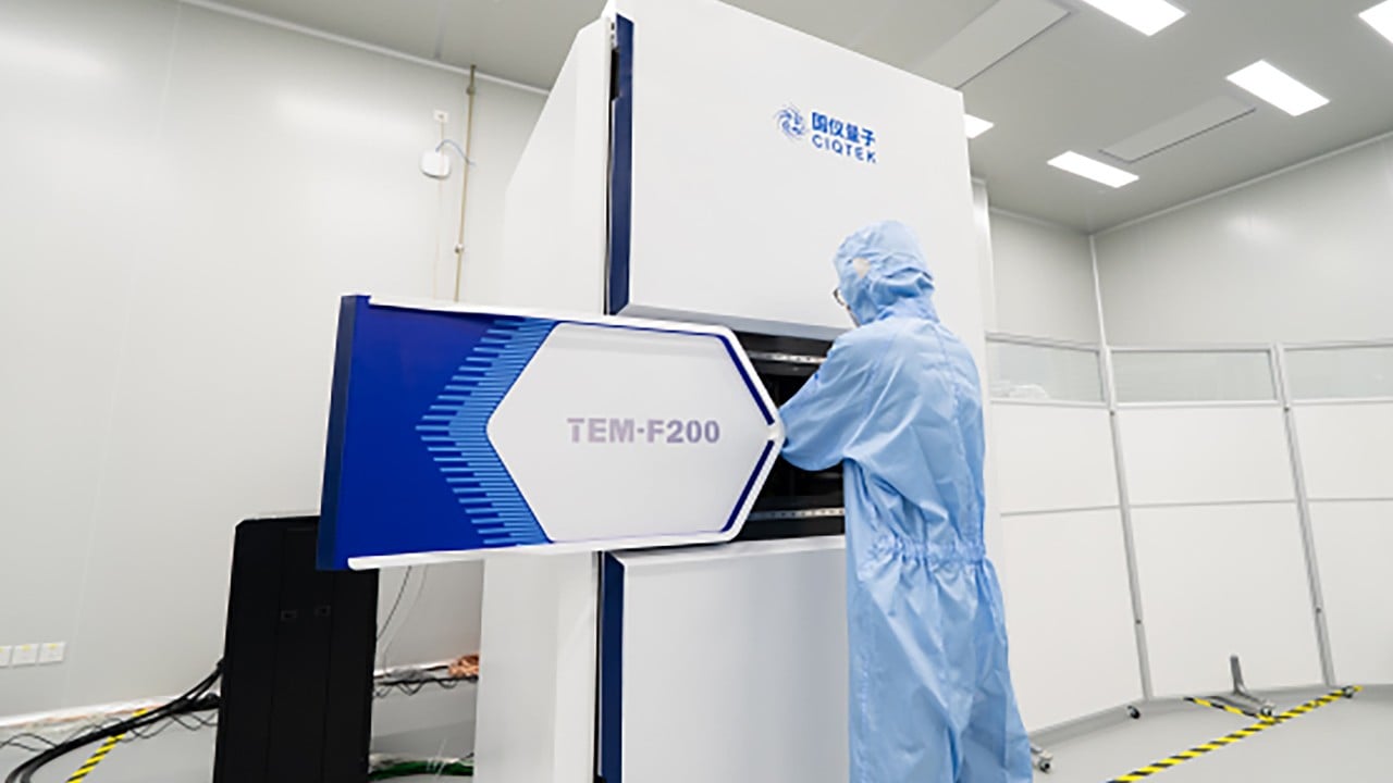
China is ready to commercialise a 200-kilovolt transmission electron microscope with an information resolution down to 0.1 nanometres that could introduce a new challenger into a market long dominated by the US and Japan.
Developed by Hefei-based manufacturer CIQTEK, the microscope features a point resolution of 0.25nm and an information limit of 0.1nm – on par with leading workhorse models on the market.
This marks a shift for the country’s expanding advanced electron microscopy industry from research and development to commercialisation, according to a report by the official ministry newspaper Science and Technology Daily on Monday.
It also represents the latest achievement aimed at reducing the country’s reliance on imports of the technology used in vital advanced industries like chip manufacturing.
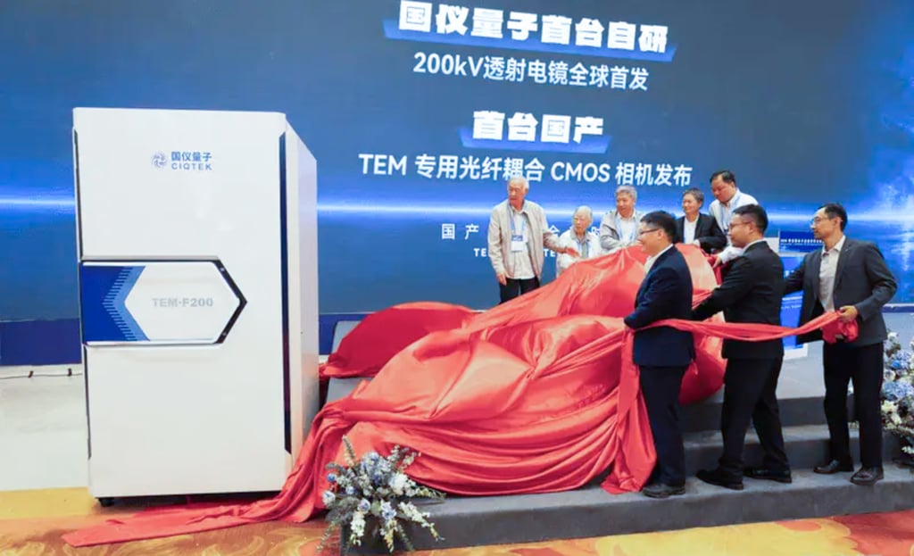
On Sunday, CIQTEK officially launched its 200kV field emission transmission electron microscope – the TEM-F200 – during the 2026 National Conference on Electron Microscopy held in Nanjing.
He Yu, CIQTEK’s chairman, described the new model as capable of supporting high-resolution imaging and defect analysis for advanced materials and semiconductors.
“Through continuous research and development, the TEM-F200 has achieved mass production and delivery capabilities,” He said, according to Science and Technology Daily.
Wu Aihua, secretary general of the China Instrument and Control Society’s analytical instruments branch, told the ministry newspaper the model could also be used in fields like biomedicine and would enhance the country’s self-sufficiency in analytical testing technologies.
The development of light microscopes throughout the 17th century enabled the magnification and capture of objects beyond the capability of human vision.
However, the resolution limit of conventional light microscopes is about 200 to 250nm, making the devices unable to visualise some of the smallest structures on Earth, including viruses and genetic building blocks.
In the early 1930s, German scientists built the first working electron microscopes, unlocking the ability to visualise even smaller structures.
Electron microscopes send focused beams of electrons rather than light at or through specimens. Detectors then capture these particles to build an image, allowing us to view details near or down to the atomic level on a display.
Modern universal workhorse electron microscopes typically operate at a 200kV accelerating voltage, which helps balance trade-offs between resolution and sample damage.
Transmission electron microscopy (TEM), one of the most common forms, uses a broad electron beam that passes through a thin sample to project an image onto a detector, according to US supplier Nanoscience Instruments.
Many modern TEM models are also capable of scanning transmission electron microscopy, which adds a tightly focused beam that scans point by point, making it easier to build high-contrast atomic images and map the composition of materials.
It has become a major part of fields like materials science, life science, as well as nano- and atomic-scale manufacturing, such as the production of chips.
05:23
China’s super microscope shows how electroacupuncture calms inflammation
The global market for commercial TEM is dominated by a handful of companies based in the US and Japan.
This includes market leaders Thermo Fisher Scientific – an American research supplier that produces its transmission electron microscopes in the Netherlands – and Japanese precision instrument developer JEOL.
Both companies produce widely used flagship 200kV transmission electron microscope models with information limits of about 0.11 to 0.12nm.
Other major players include Japanese manufacturer Hitachi and American manufacturer Bruker, whose acquired Nion series includes dedicated scanning transmission electron microscopes with world-leading resolutions.
The point resolution is the finest detail that can be directly interpreted from a microscope image. The information limit is the greatest detail the microscope can actually capture, which can be brought out using processing software.
For decades, China relied on imported TEM technology to meet its research and industrial needs. High-quality machines can cost anywhere from hundreds of thousands to millions of dollars.
In 2024, Guangzhou-based research institute Bioland Laboratory built the country’s first commercial field emission TEM, a 120kV model called the TH-F120 that is manufactured and sold by CIQTEK.
Last year, Suzhou Bozhon Instrument Technology unveiled China’s first commercial 200kV TEM model, the BZ-F200, according to a Science and Technology Daily report.
On Monday, CIQTEK announced that it had released a 120kV model called the TEM-F120, saying it could be used for life sciences and materials research.
KioskNews shows a cleaned-up reading view extracted from the publisher’s page — the original always lives on their site, not ours.